Going Open Source CAD
As can be seem from various post's here, I'm an Altium user. I'm lucky enough to have access to it work, and I've been using it since it was good old Autotrax for DOS. Yes, I'm that old....
For work that's fine but with my home projects I'm keen on sharing these as Open Source Hardware and releasing designs in Altium goes against the grain here - the community prefers that you share using open source tools.
So with this in mind, I decided to take the plunge and try KiCAD. My following thoughts will be comparisons between 'what I know' about Altium and what my impression are about KiCAD and I fear it will be far from fair. Altium does set the bar, and thus my expectations of what a PCB CAD tool can do, pretty high...

It Can Be Done!
And besides, I need something to do while I wait for my next revision of Alarm PCBs to land....
This Isn't Windows
So, rather than mucking around with bleeding edge DIY builds, I grabbed the latest Windows installer from KiCAD's site and fired it up.
My first impressions are that it's light, and fast to open. I'm using it on a 5 year old laptop, running Windows 7 with only 3GB of RAM, and t's quick and snappy. Woohoo. This laptop is capable of running the latest version of Altium, (which takes about 2 minutes to load all the features I don't use) but isn't exactly quick at it, and it's refreshing to see how quick KiCAD is.
However, rather than read the instructions I just jumped straight in to give it a go, and got no where fast. This isn't KiCAD's fault, it's just that it's different to Altium and I needed to work out my new work flow.
The other thing to consider, is that KiCAD is supported on many platforms, not just Windows and thus 'Windows Like' operation is just not going to happen. What do I mean by that?
Bye Bye Copy and Paste
Everyone who uses Windows knows the drill with Copy and Paste. Drag and Select, right click and chose copy / paste as required. Altium does that, KiCAD doesn't.
In KiCAD you drag and select, and then you are moving your selection immediately. I'm not saying this is wrong or a bad thing, it's just different to what I'm used to.

Drag and Right Click
Adding to the unfamiliar feel is that Ctrl+C (standard copy shortcut in Windows) is a 'Save Block' command in KiCAD. This is equivalent to 'group' command in Altium where you lock a set of primitives into a single group that can then be moved around easily.
This I really don't like, but I don't know if this is typical of use in a Linux or Mac Environment, or even if it's similar to AutoCAD commands (a tools who's black arts are completely unknown to me).
Order of Operations
In Altium, if I want to Edit the parameters of a part, I just have to double click it. KiCAD supports this too, so great. KiCAD will also let you edit a part via the hot key 'E' but (imho) does it the wrong way around. You need to hover your cursor over your part of interest, and then press the 'E' key. If you move the cursor off, your out of luck. To me this is awkward as I'm used to being able to mouse over a part and select it, and then chose an edit (or other) action with the part.
Again, I'm not saying this is bad or wrong, but it does add to the learning curve, especially if you're a Windows user.
Modular Operation
KiCAD does remind me of good old Autotrax in that each module operates independently of each other, rather than in an integrated manner like Altium. There are different programmes that are launched from the main KiCAD window for each stage in the PCB design:- Eeschema, the schematic editor
- PCBnew, the pcb editor
- Gerbview, the Gerber viewer
- Vcpcb, the footprint linker (between schematic parts and pcb modules)
Libraries and Parts
Also, within Eeschema is the Library Editor where you can create and edit footprints.
To get started with my KiCAD build, I decided to create a few library parts, beginning with the MAX4239 Opamp. As this is a new project, and as I'm new to KiCAD I didn't want to ruin any of the existing libraries so my instinct was to create a new one. Again, in the windows way I selected the file menu and ... WTF? No 'new' option??

Where's New?
Now, to be frank, this just pisses me off. If you launch Eeschema, the New option is there so menu behaviour is not consistent. To make a 'new' library the only way I can figure out how to do this (please feel free to correct me) is to open an existing library and then export the current part to a new library.
The Library Editor is _very_ unintuitive. Thank God for Chris Gammel and his Getting to Blinky series.
To acully be effective in the Library Editor you need to:
1. Set your current Library of interest (File , Current Library) and the following dialog pops open.

2. After selecting your Library, you still have a blank working space. You now need to either:
- make a new component

- or load an existing component

There is a built in Library Browser in the Library Editor, but selecting it DOES NOT let you select a part for editing.

Once you've loaded a part for editing it's pretty straight forward. Rather than having to memorise a bunch of hotkeys (i.e. P P for Place Pin) in Altium, the tool bars to the top left and right of the editor give you all the features you need to create your new part.

An absolute bonus is that to make a part display as Active Low (i.e. have a bar above the pin name) you simply prefix the pin name with a tilde (~). In Altium you need to prefix each character with a slash (like /t/h/i/s).
One thing that took me a while was working out how to fill the body of my part. You need to edit the 'poly line' that defines your part outline. Again, place the cursor on the poly line and hit the 'E' key.

Select 'Fill background' and you're good. And just like Henry Ford, you can have any colour you want as long as it's black yellow.
One really great feature of Altium that's not supported by KiCAD is that you can select multiple pins and edit them in a list (like a spreadsheet). This makes setting up 100 pin parts quick and easy - in KiCAD you need to edit each individual pin. Not a deal breaker by any stretch of the imagination, but not as nice as the MegaBuck professional software.

So after all that, you have a component. This is where Altium and KiCAD part ways significantly.
In Altium, you can assign a footprint to the schematic part, and when you import your design into the PCB the footprints come across easily. Whenever you place the part on the schematic, the footprint is set with it.
In KiCAD, this isn't the case. When you place your part in your schematic, there isn't any footprint information carried over with it. You need to use the Cvpb tool to assign footprints to parts outside of the schematic editor. For small part count projects, I don't see this as a problem, but I will be annoyed if i had to do this for 300 odd resistors and I need to remember which one is the high power 1206 and not a og standard 0603... Good part names / comments here would be useful.
You can add a 'footprint filter' in the library editor (you get there by double clicking within the part editor window, or by using the correct top toolbar icon ) - for example selecting SOT23 for the MAX4239

Only lets you chose footprints with SOT23 in their name when running Cvpcb.

Of course,this now means I need to make 0402, 0603, 0805 and 1210 resistor models in my library - but that's okay as I did the same thing in Alitum. Again, I'd give the win to Alitum here, but KiCAD is the right price so I can put up with this quirk.
Once you have a component loaded, you can make a new one from the one loaded (using the top tool bar) and you can export your current part to an SVG file which you can then import to a different part.
And this is the biggest kludge that hurts my brain with KiCAD. As you cannot simply copy one part in a library and then paste it in another, you need to use the import / export SVG file to copy between libraries. THIS IS A MAJOR PAIN IN THE ASS and Altium absolutely trumps KiCAD here.
Part of my distaste about this method is that it is not obvious. SVG (at least me me) suggests a vector picture file, as opposed to 'buffering' a part. Also the Import / Export *component* icons in the top toolbar are the same icons as the import / export *svg* icons in the right toolbar. WTF, confusing.
But at the end of the day it works. If you hold your tongue at the right angle.
Schematic Entry
Again, the lack of 'Windows like' features took some adjusting to to get used to, and to move parts you need to hover your cursor over the part and then hit the move hotkey ('M'). 'R' will rotate your part as well, and 'W' will start a wire from your current cursor position. This last feature is the one I stumble over the most. In Altium you can 'P W' (place wire) and then click on the starting point. This habit will take some time to break....
KiCAD is also fussy with your wire ends. You must but wires up to each other, not overlap them (otherwise the two ends are not considered to be connected). Nasty.
When I started with KiCAD it took me a week of evenings in front of the TV to work out how to build my library parts and start my schematic. After a few nights off, I decided to clear my head of prejudices I'd formed in this period and take a crack at a new design. As I was a bit foggy I didn't want to come up with a new design of my own, so in a shameless effort to draw more traffic to this blog, I decided to port a small working project to KiCAD rather than start one from scratch, and as I'm a fan of the EEVBlog I decided to take a crack at 'porting' his Rev5 uCurrent.
Dave gave me his permission (via a PM on is forum) with his only request that I remove his name and logo so that people don't think the KiCAD result is from him (and I guess so that he doesn't have to support any mistakes I introduce!).
Beawdy Dave, thanks.
So starting from scratch, in less than two hours I generated all my new library parts (only four) and then in about 90 minutes I punched out the schematic shown below.

At this point the schematic isn't complete:
- Part Values are incorrect
- Not all parts have correct footprints (yeah, my workflow is hard waired to think that footprints are a part of schematic creation)
- Parts are not annotated correctly
At the end of the day, I was pretty impressed that I was able to punch this sheet out in the one evening. Hmm, this KiCAD stuff isn't too shabby afterall....
The Cunning Plan
At this point, the efficiency bug (i.e. laziness gene) bit in. I need to create some part footprints, but they are already there in the Altium files that Dave used to produce his uCurrent.
If only there were some way I could import Dave's work into PCBnew....
Gerber Time
KiCAD has a built in Gerber Viewer and Dave's Gerbers provided in his release loaded perfectly in KiCAD!

Looking Good!

Gerber Export
Even better, GerbView has the option to export the Gerber Files to PCBnew format. This is looking good! However, opening the generated .brd file sunk these plans:

Dammit.
The text that rendered fine in the gerber viewer didn't import at all well. But at the end of the day, text is easily reproduced.
The real deal breaker is that each and every pad rendered as a through hole pad, not single layer SMD pads. Grrr. It's not obvious in the above picture, but the white circles in each pad represents a hole. This is made very clear in the 3D view.

Not Dead Yet
In getting this far in KiCAD I'd recalled seeing something about P-CAD import being available in KiCAD. I won't go on too much about the time I lost thinking I needed to compile a new version of KiCAD (as there isn't a P-CAD import option in PCBnew), but I was chuffed to find out that you can just *open* a P-CAD design in Ki-CAD.

But how is this helpful?
Altium can save a .pcbdoc in P-CAD format. WIN! To test the theory I opened this little adaptor I'd designed in the past:

I saved this as a P-CAD file in Alitum and then opened it in Ki-CAD.

WIN!
So I repeated the method with the uCurrent board:
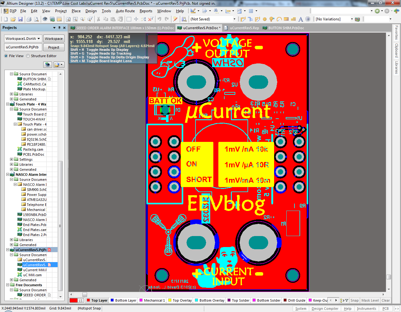
uCurrent in Altium

and failed miserably....
Thankfully the error message gave me the tip - there were some pads with zero hole size in the uCurrent design. It wasn't too time consuming to find these (in Altium you can find like objects, and I was able to filter on pad, zero hole size) and attempting the export to P-CAD / KiCAD cycle ...

.. ended in success! Yes!
Text still fails to render, but this is easily added to alter, and the slots in the binding posts came out as round holes. There is a work around to produce slots in KiCAD that I will apply later.
So this is where I'm currently at, and I'm still some way from completion. I need to:
- Make sure the imported layers are as expected (e.g. that the silk scree isn't on the solder mask layer)
- Make sure the part annotation in the schematic matches the part annotation in the imported board files
- Grab parts from the imported board and build a footprint library so I can match schematic parts to the board parts
- Work out how to match nets from the schematic to the PCB
- Fix the text.
I know I can import a board in Altium and align it with a new schematic (been there before) but can I pull this off in KiCAD? And if I can define a path to convert Altium to KiCAD, do I really need to release my designs in KiCAD or can I continue to release using Altium?
I'll let you know how I get on. Stay tuned.
FYI you can do the over bar in Altium with just the initial backslash '\'. Nice post, made me think twice about using KiCad for home projects...
ReplyDeleteThank you for this post. It was entertaining and has made me thing about how much of a pain it would be to move from Schm to PCB with the footprint select for each component.
ReplyDeleteWhen you import projects from Altuim to KiCAD dose it link the schm and the PCB files together and if you want to edit the schm will it update the PCB with out giving you 1000's of errors?
Thank you for the post make my laugh a few time. "If you hold your tongue at the right angle."
Hello Ludzinc.
ReplyDeleteI have read your article (3 times), since I am in the same circumstances as you, and with your post I have seen a ray of light.
I have followed your steps and I have had the same problems that you describe when you use gerber translation.
On the other hand, I discovered an Altium-Kikad translator in Github that I think you may be interested in not having to use PDFs for schematics and to be able to deliver a complete project in Kicad: https://github.com/thesourcerer8/altium2kicad, de " thesourcerer8 ". With the ShcDoc it works correctly, but with the PcbDoc pads it gives some problems.
I have thought to use your method Altium-> Pcad-> Kicad for the PcbDoc and the method of "thesourcerer8" for the SchPcb, but I can not get Kicad to read the export to PCAD from Altium (neither of Protel99), that I also manage (I also carry many years in this of electronics).
Please, can you explain in detail how you do to read pcbs on PCAD from Kicad?
Thank you very much.
David
email: djimelec@gmail.com